| |
Chapter 10
Verification Architecture
for Pre-Silicon Validation
Introduction
The dramatic increase in the number of gates that are available in modern integrated circuits coupled with the use of IP cores and advances in design re-use methodologies are contributing to larger, more complex and highly integrated designs. This increase in complexity results in designs that take increasingly more effort and time to verify. As explained in earlier chapters, verification tasks commonly accounts for 50% to 80% of the chip's development schedule.
RTL (Register Transfer Level) coding in Verilog and/or VHDL is the implementation methodology of choice for most chips. RTL simulation is the most common verification methodology for these chips. This chapter outlines how dynamic simulation based pre-silicon validation can be performed with a well thought out, proven verification architecture.
First of all, let us first consider the following facts:
It takes an inordinate amount of time to build the test benches (a.k.a. "test jig") to test every level of integration starting at the module level. Even if the modules are thoroughly tested in their own right, integration verification is mandatory and is a daunting task. A chip may have standard bus or interconnect interfaces and interface verification is a difficult task. A chip may have to work with other components in the system and unexpected system component interaction can result in system failure.
As a result we observe that, in real practice, most chip development groups perform some module-level verification, preferring to spend their time in full-chip or system-level verification. While 70% of the chip development time is spent in verification, 65% of that verification time is spent in the following three activities:
When we analyze where the verification time is spent we notice that verification has three major components:
Test creation and results checking take up the majority of time spent on verification. Test execution time varies greatly depending on the type of design, the simulator or hardware emulator used. In the case of hardware emulators there is an overhead in compiling and maintaining the hardware that needs to be traded off with the raw performance achieved in simulated clocks over software simulators.
Raw performance in terms of the numbers of clocks per second simulated does not necessarily translate well into a high-quality verification environment. Designers need to focus on quality instead of quantity of simulation. This means that a designer needs to consider how high-quality tests can be manually or automatically created and what trade-offs can be made.
The key objective of the verification effort is to ensure that the fabricated chip works in the real environment. Quite often development groups wait until prototypes are built in order to find out if this objective was met in a phase called "prototype validation". The cost of not having met this objective can be very severe.
This chapter outlines a strategy for pre-silicon validation that has been used by many blue-chip development groups to successfully deliver first-pass shippable silicon.
While first-pass shippable silicon also requires that circuit, timing, package and such other aspects of implementation are correct as well, we also need to consider functional verification and validation. Functional verification is one of the primary tasks that normally consumes the major amount of time and effort for the development project group.
Pre-silicon Validation
Pre-silicon validation is generally performed at a chip, multi-chip or system level. The objective of pre-silicon validation is to verify the correctness and sufficiency of the design. This approach typically requires modelling the complete system, where the model of the design under test may be RTL, and other components of the system may be behavioral or bus functional models. The goal is to subject the DUT (design under test) to real-world-like input stimuli.
The characteristics of pre-silicon validation are as follows:
Outlined below are the major considerations for a pre-silicon validation strategy.
Concurrency
Most complex chips have multiple ports or interfaces and there is concurrent, asynchronous and independent activity at these ports in a real system. A system-level verification environment should be able to create and handle such real-world concurrency to qualify as a pre-silicon validation environment. Concurrency needs to be handled in both the test controller and the bus/interface models used.
Some models will return data when a transaction completes, so the test controller or environment can do data checking. Other models require the expected data to be provided up front so the model can do data checking when the transaction completes. Such behavior impacts the test checking methodology and the amount of concurrency that can be generated.
While it may be relatively easy to generate activity or stimulate the different ports or interfaces of a chip, the difficult part is to implement an automated results or data checking strategy. In a system-level pre-silicon validation environment, designers are relieved of maintaining or keeping track of the data in test code, simplifying the task considerably for a multi-ported system.
Automated Test Generation
One must first consider the test creation and/or generation methodology. The test generation methodology is closely interrelated to the results checking strategy. For example, will you dynamically check the results while the test is running, or will you post-process the results? The answer to this question quite often depends on the type of application where the chip is being used.
Utilizing the generate/run/post-process method in a design with concurrency requires extensive intelligence of the checker or a very detailed reference model that resolves all of the ordering and predicts the final state of the system.
A dynamic test generator and checker are more effective in creating very interesting, reactive test sequences. They are more efficient because errors can be detected as they happen. In a generate/run/post-process method, one may run a simulation for eight hours, only to find during the post-process checking that an error occurred 20 minutes into the simulation, with the balance of the simulation time being useless.
In directed testing, users specify the sequence of events to generate. This is efficient for verifying known cases and conditions. Pseudo-random testing is useful in uncovering unknown conditions or corner cases.
Pseudo-random test generation, where transactions are generated from user-defined constraints, can be interspersed with blocks of directed sequences of transactions at periodic intervals to re-create real-life traffic scenarios in a pre-silicon validation environment.
Dynamic test generation also facilitates reactive test generation. Reactive test generation implies a change in test generation when a monitored event is detected during simulation.
Robust, High-quality Verification IP
The quality of verification, and therefore the probability of shippable first-pass silicon, is greatly enhanced with robust, high-quality verification IP, which includes such items as BFMs (bus functional models) and protocol monitors.
A common mistake is to require the project group that develops the RTL to also create the verification IP used to verify the RTL. While this is sometimes required for proprietary interfaces, it runs the risk of making the same wrong assumptions. Further, the rate of maturity of an internally developed model is much slower than a commercial model that has been used by multiple independent design groups, provided the supplier is responsive and diligent in increasing the model quality from its customer feedback.
Whether the design team builds or buys the verification IP, they must ensure that the models can fit into the test generation and checking strategy that is adopted. Also, the models need to operate in a mode that fits into a pseudo-random test methodology. Models that load and execute a pre-compiled test sequence do not work in an environment where a designer dynamically generates and check tests.
Models must operate at the appropriate level of abstraction, concurrency and programmable controllability:
Some processor BFMs simply drive transactions on the bus, but do not automatically handle deferred transactions and retries. They have no concept of cache coherency. The test generator, or some layer of intelligence added by the user, has to handle all of the bus-specific details that could affect the order of transaction completion, and thus, the final "correct" data values.
Some models can generate multiple transactions concurrently; some perform only one transaction at a time. Models that generate multiple transactions simultaneously may complete these transactions in an arbitrary order depending on bus timing and other concurrent traffic. If the completion order is non-deterministic, then the test generator will have to gain visibility into the system to determine the final state.
Some models represent "real" devices, and always generate or respond to signals on the bus with the same timing. To fully validate adherence to a bus protocol, the system must be tested with all possible variations in cycle timing that is allowed by the device specification. This means that the test generator should be able to change the timing of the models, and to randomly vary delays and cycle relationships, such as data wait states and snoop stalls.
Ease of Use
With the considerable pressure that is already applied to shortening the timescales that are used on most projects, design teams need to focus on completing designs and delivering shippable chips. It therefore does not make much sense to send design engineers to a training class in order to learn a new language or methodology to implement a verification strategy. A better alternative is to have a verification environment that is easy to use and intuitive as this will have a dramatic effect in increasing a designer's productivity level.
Leveraging Design and Application Knowledge
A general system-level verification environment may generate many impertinent scenarios or false errors. It is necessary that the verification tool or environment be capable of leveraging application-specific knowledge so that only the pertinent application space is tested.
Right Level of Abstraction
When a problem is difficult to solve, changing the level of abstraction at which the problem is viewed often is the key to solving it. The complexity of today's chips makes it impossible or extremely arduous to deal with bit-level signals in an interface. It is necessary to operate at the transaction level or higher level of abstraction.
Debugging
The manifestation of a problem occurs further down in simulation time from the root cause, because of the time it takes to propagate the flaw to an observable point. Ideally, but not always practical, it is best to catch a problem closer to the root cause. So, a verification environment should facilitate analysis and make it easy to trace back to the root cause of the problem.
Configurability
A system-level pre-silicon validation environment should be easily configurable, since multiple different configurations will need to be tested for a thorough system-level verification.
Reusing the Test Environment
A well-thought-out verification strategy will consider re-use of tests and the verification environment for successive revisions and generations of chips. Since test creation is one of the most time-consuming and labour-intensive parts of the verification process, designers should consider leveraging on subsequent projects the verification environment and the test suites already developed.
Machine Cycles Become Less Expensive
Many companies are using server farms to operate a verification environment that runs for 24 hrs a day 7 days a week. Linux-based server farms appear to be cost effective and easy to manage. Load balancing requirements can be easily solved with commercial tools.
Quite often, the progress in a chip development project is fix-rate limited early in the design, and as the design stabilizes, progress becomes find-rate limited. The server farm operating on a 24 x 7 basis is most useful in the find-rate limited phase of the project.
In lieu of server farms, some companies use hardware-accelerated simulation where the RTL and some portion of the test bench is mapped into gates inside an emulator or hardware accelerator. Ideally, the maximum speed-up in simulation performance will be achieved if the entire RTL and test bench is mapped into hardware. However, a completely synthesizable test bench is not always practical or effective.
When considering hardware-accelerated simulation, it is important to consider what parts of the test bench will be in hardware, what parts will be in a software simulation environment, and how the two will communicate. It is also possible to map transactors, or bus functional models, into hardware while keeping the test controller in a software simulation environment.
Whether utilizing a server farm or hardware accelerated simulation, it is important to consider upfront how the test execution machine will be kept supplied with different and interesting stimuli to simulate. An automated test generation environment or tool is imperative.
An Architecture for Pre-silicon Validation
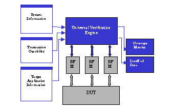
To perform pre-silicon validation, a designer needs to consider the verification architecture and the verification components necessary. To facilitate reuse and extensibility, the verification environment should be flexible enough to utilize different models for a plug-and-play, modular architecture.
Figure 10-1 shows a pre-silicon validation architecture that has been successfully used by major companies over a number of years.
Verification components
The major components for this verification approach are:
Intelligent Bus Functional Models
An intelligent BFM provides a transaction-level API, and is designed to handle concurrency and parallelism. This makes it suitable to be used in an automated test generation environment. It provides a consistent programmer's view. It also offers a high degree of controllability for the model behavior to emulate a real device with real operating characteristics through programmable delay registers and configuration registers.
Intelligent Bus Protocol Monitors
An intelligent bus protocol monitor provides dynamic protocol checking and can be used in automated test generation environments. It provides dynamic bus state information, which can be used to provide dynamic feedback to user tests or automated test controllers. It should also be extensible to accommodate user-defined sequences.
Intelligent Test Controller and Data Checker
An intelligent test controller utilizes BFMs and transaction generators to create constraint-based concurrent sequences of transactions at the different interfaces of the design under verification. An intelligent test controller can generate transactions pseudo-randomly, for a user specified sequence, or a mix of both. It can also perform specific tasks or dynamically reload input constraints upon a certain event occurring during simulation. In addition to test stimuli generation, an intelligent controller also provides for automated and dynamic data checking.
Conclusion
System-level verification requires a well thought out, proven strategy to achieve shippable first-pass silicon. This chapter has outlined the key features to consider about a system-level verification environment and the key components of a verification architecture to achieve pre-silicon validation with the ultimate goal being shippable first-pass silicon.
|
|
|