Bit-Slice Design: Controllers and ALUs
by Donnamaie E. White
Copyright © 1996, 2001, 2002 Donnamaie E. White
- Pre-Introduction
- Selection of the Implementation
- Microprogramming
- Advantages of LSI
- The 2900 Family
- Language Interrelationships
- Controller Design
- Constructing the CCU
- Sequential Execution
- Multiple Sequences
- Start Addresses
- Mapping PROM
- Unconditional Branch
- Conditional Branch
- Timing Considerations
- Pipelining
- Improved Architecture
3. Adding Programming
Support to the Controller
- Expanded Testing
- Subroutines
- Nested Subroutines
- Stack Size
- Loops
- Am29811
- Am2909/11
- CASE Statement (Am29803A)
- Microprogram Memory
- Status Polling
- Interrupt Servicing
- Implementation - Interrupt Request Signals
- Vector Mapping PROM
- Next Address Control
- Am2910
- Am2910 Instructions
- Control Lines
- Interrupt Handling
- Am2914
- Interconnection of the Am2914
6. The ALU and Basic Arithmetic
- Further Enhancements
- Instruction Fields
- Instruction Set Extensions
- Sample Operations
- Arithmetic -- General
- Multiplication with the Am2901
- Am2903 Multiply
Evolution of the ALULast Edit July 11, 2001 Adding FlexibilityThe scratchpad memory B port is connected to the B port of the ALU, to the main memory, and to the data output bus. The A port is connected to the A port of the ALU and also to the status-generating logic for input to the CCU. Note that either the A port or the B port of the scratchpad memory could have been connected to the data output bus. Input MUX AThe A port of the ALU receives input from the data input bus or the scratchpad memory A port; therefore these devices must be tristate. Assume that all input devices already are tristate. This leaves the tristate requirement for the scratchpad memory output. By adding an input MUX to the A port of the ALU and controlling this MUX from the CCU, the tristate requirements for the scratchpad A port is removed (Figure 5-6). Figure 5-6 Adding Status Flags |

| Cout | CARRY OUT, Cn + 1 |
| SIGN | Cn + 3 |
| OVR | Cn + 4 EXOR Cn + 3 |
| ZERO | Di = 0, i = 0, ..., n-1 |
These would be connected to the condition MUX of the CCU constructed earlier.
Shift and Rotate
While the ALU is capable of most operations, the ability to shift right or left ot to rotate right or left is a desirable feature. This can be accomplished by the addition shown in Figure 5-7, where a shift register has been added to the scratchpad input. The shift register is under CCU control. External connections determine whether a shift or rotate is being performed and what bit, 0 or 1, is shifted into the high or the low-order bit. A shift MUX wil be needed for each side of the ALU, which will also be under CCU control.
Figure 5-7 Adding the Shifter at the RAM input
Control Bits
Each item added which requires CCU control adds a field to the microinstruction format. The width opf the field added is a function of the amount of flexibility of the device. For a shift MUX, a 2- or 3-bit field is required. The ALU so far requires a 3-bit function field, a carry-in field (or a carry-in MUX control field), A address and B address fields of 4 bits each for fixed register operations, MUX select bits to allow A and B register addresses to be supplied from either the microinstruction register or the machine-level instruction in the IR, and controls for the A portinput MUX, the ALU output MUX, and the shift register. The microinstruction fields required by this version of the ALU are shown in Figure 5-8.
Figure 5-8 ALU portion of the microword (simple system)
|
o o o
|
Output
MUX Select |
ALU
A Port MUX Select |
Function |
Carry-In
|
A Address
|
B Address
|
A, B MUX
Select |
RAM
Shift |
o o o
|
|
1
|
1
|
3
|
1
|
4
|
4
|
1
|
2
|
Double Precision
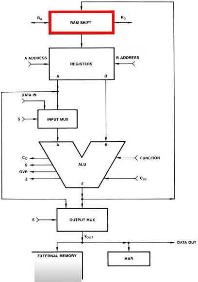
The simple system under development has no multiply or divide operations. To provide the capability for these operations, the ALU must have at least one double precision register. FOr the system developed so far, this is provided by adding an extewnsion Q register and its own shift register. The ALU inputs to the Q register directly. The Q shift register is connected to the output of the Q register. The Q register output also connects to the B port of the ALU.
To avoid requiring a tristate register and a tristate scratchpad memory, a MUX is added to the ALU B port input and the MUX is under CCU control. External connections determine the shift or rotate operations on Q alone or Q and a scratchpad register. The addition is shown in Figure 5-9.
Figure 5-9 Am2901 ALU

Additional Modifications
A few additional improvements can be made:
First, adding a zero input to the ALU A and B port input MUXs allows incrementing and decrementing as well as PASS operations on both ports.
| B + 0 -> B | PASS |
| B + 0 _ Cin -> B | INCR |
Second, adding the A port of the scratchpad to the ALU B port input MUX allows a fast multiply by 2:
| A + A -> A | MULT 2*A |
Third. adding an output enable control and making the ALU output MUX into a tristate MUX allows the ALU to share a bus.
Finally, adding two additional status outputs, carry-generate G' and carry propogate P' , allows fast addition using a carry-look-ahead if the ALU is assumed to be a 4-bit wide slice.
The result is shown in Figure 5-9 and is a logical block diagram of the original Am2901 bit-slice RALU. [This part is no longer in production.]