ROUTING
Once the designer has floorplanned a chip and the logic cells within the flexible blocks have been placed, it is time to make the connections by routing the chip. This is still a hard problem that is made easier by dividing it into smaller problems. Routing is usually split into global routing followed by detailed routing .
Suppose the ASIC is North America and some travelers in California need advice on how to drive from Stanford (near San Francisco) to Caltech (near Los Angeles). The floorplanner has decided that California is on the left (west) side of the ASIC and the placement tool has put Stanford in Northern California and Caltech in Southern California. Floorplanning and placement have defined the roads and freeways. There are two ways to go: the coastal route (using Highway 101) or the inland route (using Interstate I5, which is usually faster). The global router specifies the coastal route because the travelers are not in a hurry and I5 is congested (the global router knows this because it has already routed onto I5 many other travelers that are in a hurry today). Next, the detailed router looks at a map and gives indications from Stanford onto Highway 101 south through San Jose, Monterey, and Santa Barbara to Los Angeles and then off the freeway to Caltech in Pasadena.
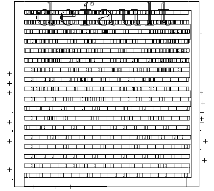
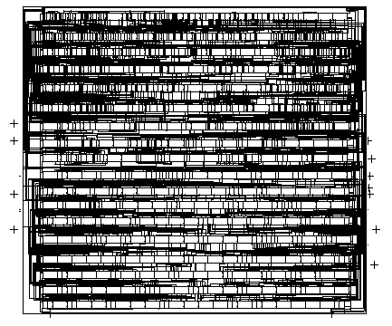
Figure 17.1 shows the core of the Viterbi decoder after the placement step. This implementation consists entirely of standard cells (18 rows). The I/O pads are not included in this example—we can route the I/O pads after we route the core (though this is not always a good idea). Figure 17.2 shows the Viterbi decoder chip after global and detailed routing. The routing runs in the channels between the rows of logic cells, but the individual interconnections are too small to see.