|
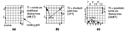
FIGURE 17.24 Examples of trees for timing-driven layout. (a) The MRST. (b) The shortest-path tree (SPT). (c) The quadratic minimum Steiner tree (QMST). (Problem 17.21 ) |
[ Chapter start ] [ Previous page ] [ Next page ]
*=Difficult, **=Very difficult, *** = Extremely difficult
17.1 (Routing measures, 20 min.). Channel density is a useful measure, but with the availability of more than two layers of metal, area-based maze routers are becoming more common. Lyle Smith, in his 1983 Stanford Ph.D. thesis, defines the Manhattan area measure ( MAM) as:
where you calculate the area needed by assuming routing on a single layer and ignore any interconnect overlaps. Calculate the MAM for Figure 17.14 . Once the MAM reaches 0.5, most two-layer routers have difficulty.
17.2 (*Benchmarking routers, 30 min.) Your design team needs a new router to complete your ASIC project. Your boss puts you in charge of benchmarking. She wants a list of the items you will test, and a description of how you will test them.
17.3 (Timing-driven routing) (a) Calculate the delay from A to C in Figure 17.3 (b) if the wire between V 3 and V 4 is increased to 5 mm. (b) If you want to measure the delay to the 90 percent point, what is the skew in signal arrival time between inverters B and C? (c) If you use the Elmore constant to characterize the delay between inverter A and inverter C as an RC element, what is the delay (measured to the 50 percent trip point) if you replace the step function at the output of inverter A with a linear ramp with a fall time of 0.1 ns?
17.4 (Elmore delay, 30 min.) Recalculate t D 4 , t D 2 , and t D 4 – t D 2 for the example in Section 17.1.2 neglecting the pull-down resistance R pd and comment on your answers.
17.5 (Clock routing, 30 min.) Design a clock distribution system with minimum latency given the following specifications: The clocked elements are distributed randomly, but uniformly across the chip. The chip is 400 mil per side. There are 16,000 flip-flops to clock; each flip-flop clock input presents a load of 0.02 pF (one standard load). There are four different types of inverting buffer available (typical for a 0.5 m m process):
1X buffer: T D = 0.1 + 1.5 C L ns; 4X buffer: T D = 0.3 + 0.55 C L ns;
8X buffer: T D = 0.5 + 0.25 C L ns; 32X buffer: T D = 2 + 0.004 C L ns.
In these equations T D is the buffer delay (assume rise and fall times are approximately equal) and C L is the buffer load expressed in standard loads. Electromigration limits require a limit of 1 mA (DC) per micron metal width or 10 mA per micron for AC signals with no DC component. No metal bus may be wider than 100 m m. The m2 line capacitance is 0.015 f F m m –2 (area) and 0.035 f F m m –1 (fringing).
17.6 (Power and ground routing, 10 min.) Calculate the parallel-plate capacitance between a VDD power ring routed on m2 and an identical VSS ring routed on m1 directly underneath. The chip is 500 mil on a side; assume the power ring runs around the edge of the chip. The VDD and VSS bus are capable of carrying 0.5 A and are both 500 m m wide. Assume that m1 and m2 are separated by a SiO 2 dielectric 10,000 Å thick. This capacitance can actually be used for decoupling supplies.
17.7 (Overlap capacitance, 10 min.) Consider two interconnects, both of width W , separated by a layer of SiO 2 of thickness T, and that overlap for a distance L.
17.8 (Standard load, 10 min.) Calculate the size of a standard load for the 1 m m process with the parasitic capacitance values shown in Table 17.2 . Assume the n -channel and p -channel devices in a two-input NAND gate are all 10/1 with minimum length.
17.9 (Fringing capacitance, 45 min) You can calculate the capacitance per unit length (including fringing capacitance) of an interconnect with rectangular cross section (width W , thickness T , and a distance H above a ground plane) from the approximate formula (from [ Barke, 1988]—the equation was originally proposed by van der Meijs and Fokkema):
where e = e r e 0 is the dielectric constant of the insulator surrounding the interconnect. The relative permittivity of a SiO 2 dielectric e r = 3.9, and the permittivity of free space e 0 = 3.45 ¥ 10 –11 Fm –1 .
17.10 (Coupling capacitance, 30 min.) One of the reasons to follow quasi-ideal scaling for the physical dimensions of the interconnect is to try and reduce the parasitic area capacitance as we scale. (The other reason is to try and keep interconnect resistance constant.) Area capacitance scales as 1/ s by following ideal scaling rules, but scales as 1/ s 1.5 by using quasi-ideal scaling. Using quasi-ideal scaling means reducing the widths and horizontal spacing of the interconnect by 1/ s and the height of the lines and their vertical separation from other layers by only 1/ s 0.5 . The effect is rather like turning the interconnects on their sides. As a result we must consider parasitic capacitances other than just the parallel-plate capacitance between two layers. The parasitic capacitance between neighboring interconnects is called coupling capacitance . Fringing capacitance results from the fact that the electric field lines spill out from the edges of a conductor. This means the total parasitic capacitance is greater than if we just considered the capacitance to be formed by two parallel plates.
The following equation is an approximate expression for the capacitance per unit length of an isolated conductor of width W and thickness T , separated by a distance H from a conducting plane, and surrounded by a medium of permittivity e [ Sakurai and Tamaru, 1983]:
where C a represents the contribution from two parallel plates and C b is the fringing capacitance (for both edges). The following equation then takes into account the coupling capacitance to a neighbor conductor separated horizontally by a gap G between the edges of the conductors:
|
C 1 / e + [0.03( W / H ) + 0.83 ( T / H ) – 0.07 ( T / H ) 0.222 ]( G / H ) –1.34 . |
where C c is the coupling capacitance from the conductor to one neighbor. For a conductor having two neighbors (one on each side), the total capacitance will be
Table 17.3 shows the result of evaluating these equations for different values of T/H , W/H , and S/H for l = 0.5 m m.
|
TABLE 17.3 Calculated fringing capacitance (per unit length and normalized by permittivity) using quasi-ideal scaling and the Sakurai–Tamaru equations. Problem 17.10 completes this table. |
||
Table 17.4 shows the predicted fringing and coupling capacitance for a l = 0.5 m m process expressed in pFcm –1 .
|
TABLE 17.4 Predicted line capacitance including fringing and coupling capacitance (pFcm –1 ) for l = 0.125 m m and using quasi-ideal scaling and the Sakurai equations. Problem 17.10 completes this table. |
|||
17.11 (**Routing algorithms, 60 min.) “The Lee algorithm is guaranteed to find a path if it exists, but not necessarily the shortest path.” Do you agree with this statement? Can you prove or disprove it?
“The Hightower algorithm is not guaranteed to find a path, even if one exists.” Do you agree with this statement? Can you prove or disprove it? Hint: The problems occur not with routing any one net but with routing a sequence of nets.
17.12 (Constraint graphs, 10 min.) Draw the horizontal and vertical constraint graphs for the channel shown in Figure 17.13 (a). Explain how to handle the net that exits the channel and its pseudoterminal.
17.13 (**Electromigration, 60 min.) You just received the first prototype of your new ASIC. The first thing you do is measure the resistance between VDD and VSS and find they are shorted. Horrified, you find that you added your initials on m1 instead of m2 and shorted the supplies, next to the power pads. Your initials are only 10 m m wide, but about 200 m m high! Fortunately only the first capital “I” is actually shorting the supplies. The power-supply rails are approximately 100 m m wide at that point. A thought occurs to you—maybe you can electromigrate your initial away. You remember that electromigration obeys an equation of the form:
where MTTF is the mean time to failure, A is a constant, J is the current density, E is an activation energy, k is Boltzmann’s constant, and T is absolute temperature. You also remember the rule that you can have about 1 mA of current for every l of metal width for a reasonable time to failure of more than 10 years. Since this chip is in 0.5 m m CMOS ( l = 0.25 m m), you guess that the metal is about 0.5 m m thick, and the resistance is at least 50 m W /square.
17.14 (**Routing problems, 20 min.) We have finished the third iteration on the new game chip and are having yield problems in production. This is what we know:
1. We changed the routing on v3 by using an ECO mechanism in the detailed router from Shortem. We just ripped up a few nets and rerouted them without changing anything else.
2. The ASIC vendor, Meltem, is having yield problems due to long metal lines shorting—but only in one place. It looks as though they are the metal lines we changed in v3. Meltem blames the mask vendor—Smokem.
3. To save money we changed mask vendors after completing the prototype version v1, so that v2 and v3 uses the new mask vendor (Smokem). Smokem confirms there is a problem with the v3 mask—the lines we changed are shifted very slightly toward others and have a design rule violation. However, the v2 mask was virtually identical to v3 and there are no problems with that one, so Smokem blames the router from Shortem.
4. Shortem checks the CIF files for us, claims the mask data is correct, and they suggest we blame Meltem.
We do not care (yet) who is to blame, we just need the problem fixed. We need suggestions for the source of the problem (however crazy), some possible fixes, and some ideas to test them. Can you help?
17.15 (*Coupling capacitance, 30 min.) Suppose we have three interconnect lines running parallel to each other on a bus. Consider the following situations (VDD = 5 V, VSS = 0 V):
How do you define capacitance in these cases? In each case what is the effective capacitance from the center to the neighboring lines using your definition?
17.16 (**2LM and 3LM routing, 10 min.) How would you attempt to measure the difference in die area obtained by using the same standard-cell library with two-level and three-level routing?
17.18 (***Standard-cell aspect ratio, 30 min.) How would you decide the optimum value for the logic cell height of a standard-cell library?
17.19 (Electromigration, 20 min.)
17.20 (***SPF parameters, 120 min.). Hint: You may need help from [ O’Brien and Savarino, 1989] for this question.
17.21 (**Distributed-delay routing, 120 min. [Kahng and Robins, 1995]) The Elmore constant is one measure of net delay,
The distributed delay , defined as follows, is another measure of delay in a network:
We can write this equation in terms of network components as follows:
In this equation there are two types of capacitors: those due to the interconnect, C 0 , and those due to the gate loads at each sink, C n . R d is the driving resistance of the driving gate (the pull-up or pull-down resistance); R 0 is the resistance of a one-grid-long piece of interconnect; and C 0 is the capacitance of a one-grid-long piece of interconnect. Thus,
since every path to ground must pass through R d . L kn is the path length (in routing-grid units) between a node k and one of the n sink nodes.
With these definitions we can expand Eq. 17.21 to the following:
Figure 17.24 shows examples of three different types of trees. The MRST minimizes the rectilinear path length. The shortest-path tree ( SPT ) minimizes the sum of path lengths to all sinks. The quadratic minimum Steiner tree ( QMST ) minimizes the sum of path lengths to all nodes (every grid-point on the tree).
|
FIGURE 17.24 Examples of trees for timing-driven layout. (a) The MRST. (b) The shortest-path tree (SPT). (c) The quadratic minimum Steiner tree (QMST). (Problem 17.21 ) |
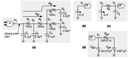
17.22 (**Elmore delay, 120 min.) Figure 17.25 shows an RC tree. The m th moment of the impulse response for node i in an RC tree network with n nodes is
|
FIGURE 17.25 Standard parasitic format (SPF) (Problem 17.22 ). (a) An RC interconnect tree driven by a NAND gate. (b) The NAND gate modeled by an ideal switch. (c) The NAND gate modeled with a pull-down resistance, R F , and output capacitance, C L . (d) The PI segment model for the RC tree (the order of C p i 1 —last—and C p i 2 is correct). |
The Elmore constant is the first moment of the impulse response. We calculate the weighted-capacitance values in Eq. 17.24 as follows:
We derive the PI segment parameters used in SPF from the k i as follows:
[ Chapter start ] [ Previous page ] [ Next page ]